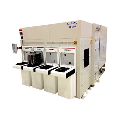
เลือกภาษาของคุณ

Product Fillter

Model: NA

Ashing System

The ashing system is available in two types: one designed for wafers and the other for panels.

The wafer-compatible model features a wafer-size-free design, capable of handling a wide range of processes from next-generation wafer processes to wafer-level packaging. It is the most widely adopted device in semiconductor packaging processes.

The panel-compatible model supports panels up to 600mm square, allowing for uniform Descum processing and Ti etching even on large panels.

Image

Features

Model: NA-8000 and 1300

  • Enables damage-free ion implant stripping and polymer removal processes.
  • The chamber configuration optimized for F-based gas addition processes allows particle-free operation. This makes it suitable for a wide range of processes, including normal PR, ion implant stripping, organic film stripping (PI, DFR, etc.), and oxide etching.
  • Simple design ensuring excellent maintenance, reliability, and cost-efficiency.
  • The option to choose from different chamber configurations (μ-wave, RIE, μ-wave + RIE) allows optimal settings based on the process.
  • Easy wafer size change through recipe settings.

Model: NA-1500

  • Selectable microwave downflow and/or RF bias.
  • Suitable for Ti seed layer etching, Descum, and surface treatments.
  • Supports new processes such as surface treatment and hydrophilization, in addition to ashing.

Applications

  • High dose ion implant stripping process (10E + 16 atoms/cm2 or higher) and polymer removal in front end process
  • Wafer process that requires CF4 addition process (electronic parts and LEDs)
  • Chip size package and bump process
  • CCD color filter manufacturing process
  • Descum, Desmear
  • Surface modification (hydrophobic to hydrophilic, hydrophilic to hydrophobic), pre-treatment for wet processes such as plating and underfill
  • Ashing of resin-based materials

Specifications

Model NA-8000 NA-1300 NA-1500
Wafer Size(mm) Φ100~200 Φ200 and Φ300 Max. 600mm square
Process chamber 1 2~6 2
Plasma Source MW、RF MW、VHF、RF
Applications R&D~Small-scale production Large-scale production Panel level packaging(PLP)